Components for combined credentials
Multi-Chip Combi Card Inlays
Independent circuits. One card body.
A combi card inlay places multiple independent chip circuits in one card body. The circuits may use the same RF band or different bands; a separate contact module is another possible architecture. Each chip keeps its own memory and application behavior. Compare the component specifications, reader selection and physical layout before qualifying a combined card.
Download technical reference (PDF) ↓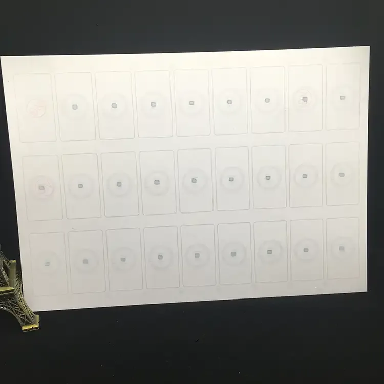
Technical overview
Chip count, RF bands and interfaces are different choices.
“Combi” describes independent circuits sharing the physical card. It does not imply one common memory or a particular frequency pair.
- Combi / multi-chip
- Multiple ICs. Each keeps its own memory and application behavior. Same-band HF + HF is possible as a design requirement.
- Dual-frequency
- Two RF bands. LF + HF is one example. A multi-chip dual-frequency design is also a combi design. Compare band pairings →
- Dual-interface CPU
- One CPU, two interfaces. Contact pads and an RF antenna address that CPU. See module and connection references →
- Contact + separate RF
- A contact module plus an independent RF chip is a multi-chip arrangement. The contact module and its cavity must be specified separately; the images here do not identify a contact CPU.
Named component references
Two combinations, with separate specifications.
These two-chip configurations are engineering references built from manufacturer IC specifications. They are not stock assemblies or evidence of RF coexistence. A quotation defines the supplied chips, antenna layout and sample qualification.
| Reference combination | Technology | Memory | Application & design implication |
|---|---|---|---|
| NTAG213 + MIFARE DESFire EV3Engineering reference | HF + HF: two 13.56 MHz ICs. NTAG213 uses NFC Type 2; DESFire EV3 uses ISO/IEC 14443-4 / NFC Type 4. | NTAG213: 144 bytes user memory. DESFire EV3: 2 / 4 / 8 / 16 kB non-volatile memory, by variant. Separate memory areas. | A candidate for a public NFC link alongside a separately managed DESFire access application.The reader must select the intended IC and use its commands. Test phone selection as well as access-reader transactions; two chips at 13.56 MHz do not guarantee the intended tap result.Discuss this combination → |
| EM4200 + NTAG213Engineering reference | LF + HF: an EM4200 coil specified for a 125 kHz reader plus a 13.56 MHz NFC Type 2 circuit. | EM4200: factory-programmed ROM, 128-bit with 64 / 96-bit options. NTAG213: 144 bytes user memory. No shared memory. | A candidate for an existing LF identifier and a separate NFC phone link in the same credential.Choose the EM4200 variant and returned ID format first. Its fixed identifier and the NFC data are linked in the application database, not automatically by the inlay.Discuss this combination → |
Memory capacities cannot be added into a common storage area. NDEF formatting and application files use part of the stated space. The chip specifications do not establish finished-card reading distance.
Same-band behavior
Anticollision selects a chip; it does not choose your business application.
NTAG213 and DESFire EV3 both use 13.56 MHz Type A activation, but their application commands differ. The terminal must select and address the intended IC. A public link on one chip does not guarantee that a phone will open that link when both chips are present.
What a combined sample must demonstrate
The access reader completes its intended DESFire transaction. The phone selects the intended NFC record. Both still work after the shared stack is laminated and punched. Antenna coupling and firmware selection are separate questions, so protocol support alone cannot qualify the assembly.
One issued card, separate identifiers
- LF system record
- Store the EM4200 value actually returned by the reader, with its formatting.
- NFC function
- Store the NTAG UID or assigned application reference alongside its encoded link.
- Issuing record
- Associate the two records with the same issued card; replace or revoke both together.
This is an application-mapping example for the LF + HF reference, not shared chip memory.
Original visual references
See the circuit arrangement before defining the production drawing.
The photograph above shows an original sheet. These two illustrations explain the repeated positions and separate connections without assigning an unverified chip model.
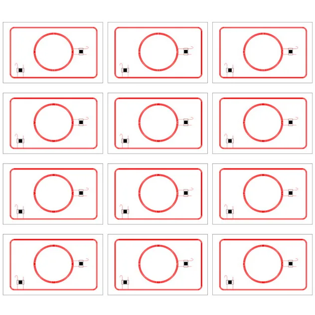
4 × 3 layout illustration
Twelve illustrated card positions. Each position depicts a rectangular antenna and a circular coil with separate components. This is a layout illustration, not a dimensioned drawing or a photographed production batch.
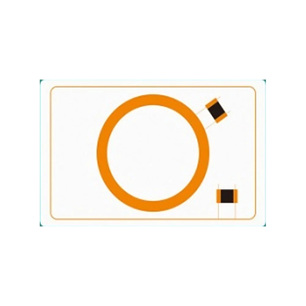
Two-circuit construction illustration
Illustrates separate antenna connections within one card outline. The drawing does not establish frequency, chip identity or interference-free operation.
Package and card clearance
Die thickness is not the finished inlay thickness.
The package, antenna attachment and cavity all contribute to local height. Start with the exact ordering code rather than applying one thickness to every chip combination.
- NTAG213 bare-die references
- NT2H1311G0DUF: 75 µm wafer thickness; NT2H1311G0DUD: 120 µm. Both are 144-byte, 50 pF references. These are die values, not inlay thickness.Manufacturer ordering table ↗
- DESFire EV3 module reference
- MF3D4300DA4/00: 4 kB, 17 pF, MOA4 / SOT500-2. The module outline and assembled bond height govern the local cavity; its memory size does not define clearance.Manufacturer ordering table ↗
Reserve space for each connection and the final cut.
The drawing needs a local section through each module, antenna-connection clearance and distance to the punching boundary. Staggering two modules changes local stack-up; it does not remove the need to measure both regions. A separate contact module also introduces a cavity and an insertion process that must avoid the RF conductors.
There is no universal clearance in millimetres for the two references above. Package drawings and the converter’s process tolerances determine those dimensions. Supplied sheet thickness, material and layout are stated on the approved production drawing.
Technical documents
Take the comparison into your engineering review.
The PDF collects the chip combinations, package references and visual evidence. It is a technical reference, not a current production drawing or qualification certificate.
Download Combi technical reference ↓Revision: 15 September 2026
Custom orders & samples
Bring the chosen chip functions into your inquiry.
Choose a reference or describe your own combination. The next step opens an editable inquiry draft so you can add readers, drawings and quantities.
Current sheet dimensions, thickness, materials, MOQ and lead time are quoted for the approved assembly. The engineering references above are not a stock list.
Combi card-inlay questions
Is a combi card the same as a dual-interface card?
A combi card contains multiple independent chip circuits. A dual-interface card uses one CPU with contact and contactless interfaces. A combi design can also contain a contact module, but separate chips do not become one shared CPU. A dual-frequency card specifically operates across two RF bands, which is one possible combi arrangement.
Will a phone automatically select the NFC chip in an HF + HF card?
Do not assume it will. Anticollision lets a reader select individual Type A chips, but the reader and application still decide what to select and which commands to use. An NTAG213 plus DESFire EV3 design needs phone tests and access-reader tests in its finished card form. Protocol support alone does not establish the intended phone-tap behavior or antenna coexistence.
Do both chips have the same card number or share memory?
Independent chips retain separate identifiers and memory. For example, EM4200 contains a factory-programmed identifier while NTAG213 has its own UID and writable user area. The issuing application can associate both with one card record. Record the actual reader output, chip assignment and replacement rules; storing one common application reference does not make the factory identifiers identical.