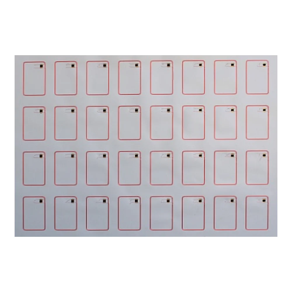
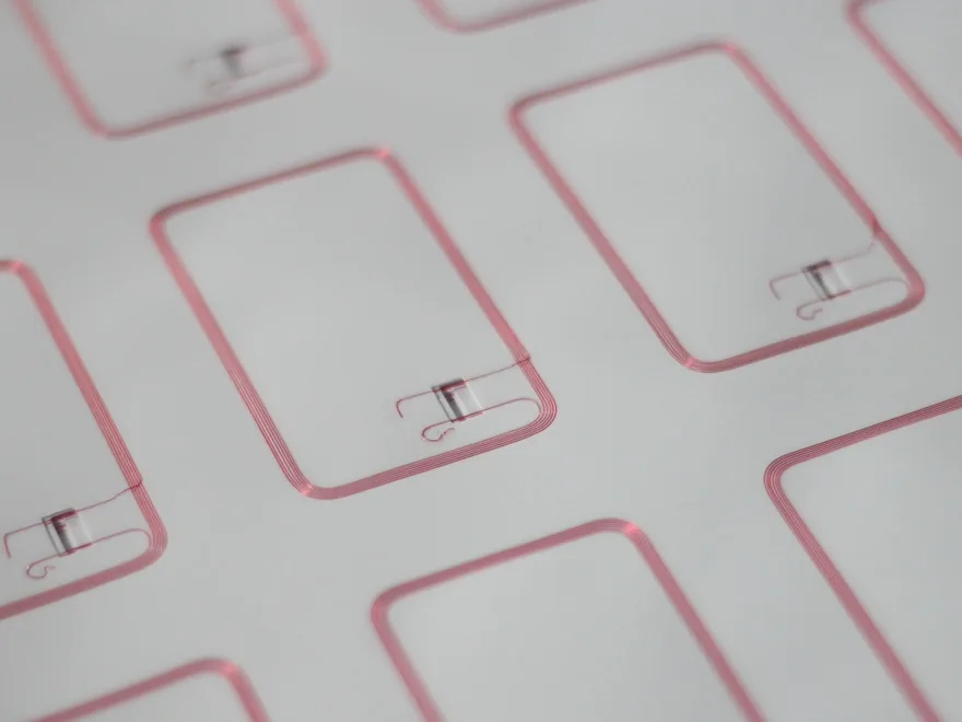
4 × 8 antenna sheet
32 pictured positions
The antenna pattern and chip positions are visible before the outer card layers are added.
Request this layout reference →Card production components
13.56 MHz chip and antenna sheets
HF RFID card inlays combine a 13.56 MHz chip and antenna in a sheet for conversion into contactless cards. NTAG, MIFARE and ICODE designs serve different phone, access-control and ISO/IEC 15693 applications. Compare the chip interface and memory below, then select a sheet layout for your card production line.
Technical overview
A chip determines the interface and memory. The antenna, sheet and card layers determine how that chip fits your production process.
Chip specifications
These are NXP chip-level references. Your quotation identifies the supplied chip, sheet construction and production availability.
| Chip | Interface | Memory | Application fit |
|---|---|---|---|
| NTAG213NXP datasheet ↗ | ISO/IEC 14443 Type A · NFC Forum Type 2 | 144 bytes user memoryRead/write area; NDEF formatting also occupies space. | NFC cards carrying a short web link or text record.Request NTAG213 quote → |
| NTAG215NXP datasheet ↗ | ISO/IEC 14443 Type A · NFC Forum Type 2 | 504 bytes user memoryRead/write area; NDEF formatting also occupies space. | NFC cards carrying a larger record or several small records.Request NTAG215 quote → |
| NTAG216NXP datasheet ↗ | ISO/IEC 14443 Type A · NFC Forum Type 2 | 888 bytes user memoryRead/write area; NDEF formatting also occupies space. | NFC cards with more information stored directly on the chip.Request NTAG216 quote → |
| MIFARE DESFire EV3NXP datasheet ↗ | ISO/IEC 14443 Type A, Parts 1–4 · NFC Forum Type 4 | 2 / 4 / 8 / 16 kB non-volatile memoryCapacity depends on the IC variant; files and application structure use this memory. | Access and multi-application credentials using a DESFire application.Request MIFARE DESFire EV3 quote → |
| MIFARE Classic EV1 1KNXP datasheet ↗ | ISO/IEC 14443 Type A activation · MIFARE Classic commands | 1 kB total EEPROM · 16 sectorsIncludes manufacturer data and sector trailers; 1 kB is not all application space. | Existing card systems designed for MIFARE Classic 1K.Request MIFARE Classic EV1 1K quote → |
| ICODE SLIX2NXP datasheet ↗ | ISO/IEC 15693 | 316 bytes user data · separate counter block80 × 4-byte blocks: 79 for user data and the final block for the counter function. | ISO/IEC 15693 cards for library, asset and document systems.Request ICODE SLIX2 quote → |
Memory figures describe different areas of each chip. NDEF formatting, application files and access-control data use part of the available space.
Sheet examples
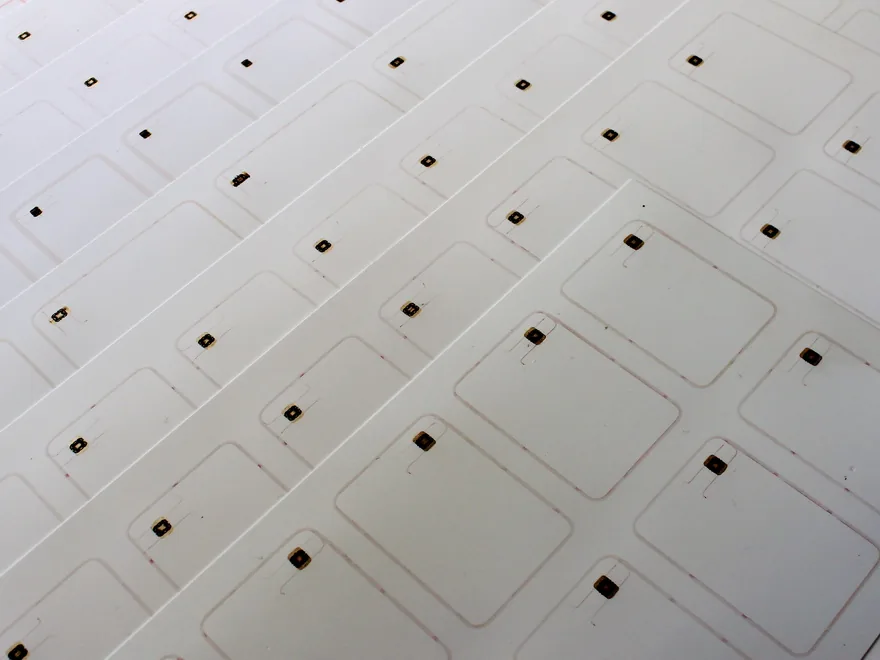
These photographed sheets show two layouts. Position counts apply to the pictured examples; sheet dimensions, pitch and the exact chip are specified separately in the order drawing.
32 pictured positions
The antenna pattern and chip positions are visible before the outer card layers are added.
Request this layout reference →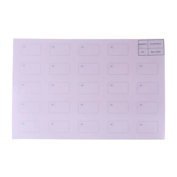
25 pictured positions
The photo label reads “M1 inlay 5*5 format” and “25pcs (1 sheets)”. It identifies this photographed example.
Request this layout reference →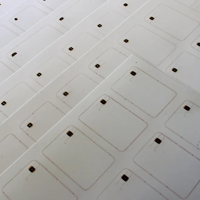
Construction reference
The antenna core and cover sheets become part of the completed card. This dimensioned example shows the difference between the inlay subtotal and the full card stack.
| Layer | mm |
|---|---|
| Front overlay | 0.06 |
| Front printing layer | 0.12 |
| Inlay top cover | 0.15 |
| Antenna core | 0.15 |
| Inlay bottom cover | 0.15 |
| Reverse printing layer | 0.12 |
| Reverse overlay | 0.06 |
| Inlay subtotal Sum of layers 3–5 | 0.45 |
| Complete card Total stated in the source | 0.81 |
COB = chip on board. The illustrated COB position is within the antenna-core area.
Source: ACT Trinnovation 2017-Q4 technical presentation, slide 21.
Historical reference example. These values describe the illustrated construction; they are not current RFIDAK supply specifications. Confirm the materials, layer stack and finished thickness on your project drawing before sampling.
Technical documents
The reference PDF contains the chip comparison, source links and the illustrated layer dimensions. Use an order-specific drawing for production dimensions and tolerances.
Download HF technical reference ↓PDF · version 15 September 2026 · technical reference
Custom orders & samples
Select the chip and layout you want to discuss. Add quantities, delivery destination and your drawing requirements on the next page.
Your quotation will state substrate, dimensions, tolerances, sample charges, MOQ and lead time. A layout reference is a starting point for the drawing.
Sample ordering terms →NTAG213, NTAG215 and NTAG216 provide 144, 504 and 888 bytes of user memory respectively. A short web link commonly fits NTAG213; longer or multiple records need more space. NDEF formatting uses some memory. Test the encoded finished card on the phones your customers use.
Inlay thickness covers the antenna core and its cover layers. The complete card adds printing layers and overlays. In the sourced COB construction example, the three central layers total 0.45 mm and all seven layers total 0.81 mm. These are dimensions of that historical example, not a standard thickness for every order.
These chips use different commands and application structures. ICODE SLIX2 uses ISO/IEC 15693; MIFARE Classic and DESFire use different application protocols within ISO/IEC 14443 Type A. Select a chip supported by the installed reader and software, including the credential data and personalization process.
May we use Google Analytics cookies to measure visits and inquiry actions? Your choice does not affect the contact form. Cookie details