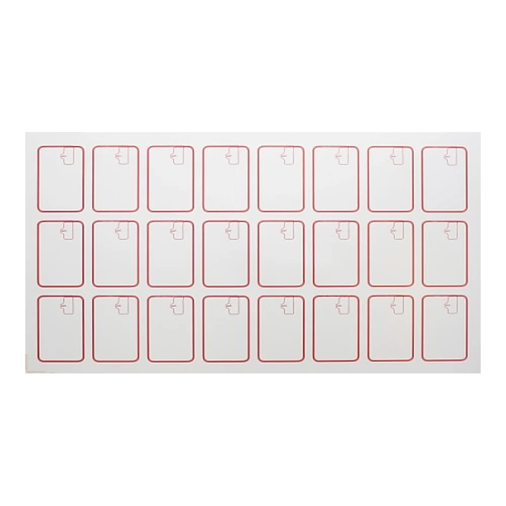
3 × 8 antenna sheet
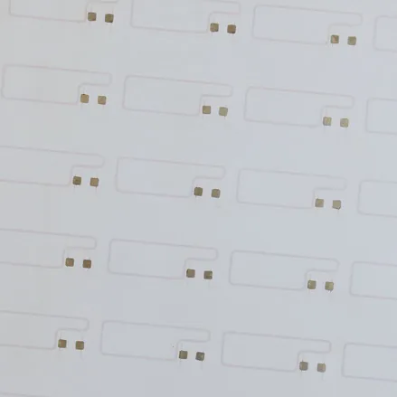
24 pictured antenna positions. This photo shows the loop and connection-area arrangement before a CPU module is installed.
CPU card production components
One CPU · contact and contactless
Dual-interface CPU card inlays provide the antenna structure for a smart card that uses contact pads and a 13.56 MHz contactless interface with one compatible CPU chip. The module connects to the card antenna electrically or by inductive coupling. Choose the connection method and module together; an antenna-only sheet does not yet contain a working CPU card.
Technical overview
The module provides the processor, memory and application. The inlay provides the antenna and the physical connection or coupling area inside the card.
NXP contact / contactless interface reference ↗Module-to-antenna connections
Four construction approaches are illustrated below. The selected CPU module and card production process determine which connection is suitable; the quotation defines the supplied assembly stage.
| Connection | How it works | Production fit |
|---|---|---|
| Soldered antenna leadsDirect electrical connection | Antenna ends are soldered to the compatible module terminals. | A production line equipped to join and inspect the antenna leads.Discuss this connection → |
| Zigzag + conductive adhesiveDirect electrical connection | Conductive adhesive joins zigzag antenna-end regions to the module. | A matching module terminal geometry and controlled adhesive bonding process.Discuss this connection → |
| Pads + conductive adhesiveDirect electrical connection | The antenna terminates at pads; conductive adhesive connects the module to those pads. | A prelam with pad positions and a module cavity aligned to the chosen module.Discuss this connection → |
| Inductive close couplingElectromagnetic connection | A coil on the module couples to the card antenna without a galvanic connection. | A compatible inductive-coupling module and a matched coupling-loop design.Discuss this connection → |
Construction references: ACT / Trinnovation Q4-2017, slides 23–26. The inductive principle is also documented by Infineon Coil on Module ↗. Illustrations explain the connection; they are not scale drawings or module-compatibility guarantees.
Dimensioned construction references
These redrawn stacks preserve the dimensions of the supplied ACT / Trinnovation Q4-2017 examples. They help compare layer arrangements; current order dimensions and tolerances require an approved production drawing.
| Layer | mm |
|---|---|
| 1. Front overlay | 0.08 |
| 2. Front printing layer | 0.13 |
| 3. Inlay top cover | 0.13 |
| 4. Antenna core | 0.13 |
| 5. Inlay bottom cover | 0.13 |
| 6. Reverse printing layer | 0.13 |
| 7. Reverse overlay | 0.08 |
| Complete illustrated card | 0.81 |
Central three-layer inlay subtotal: 0.39 mm.
Source: ACT / Trinnovation Q4-2017, slide 23. The full-card total agrees with the listed layers; the inlay subtotal is calculated from the indicated layers. These values describe the source example, not current supply dimensions or tolerances.
| Layer | mm |
|---|---|
| 1. Front overlay | 0.06 |
| 2. Front printing layer | 0.13 |
| 3. Compensation core 1 | 0.10 |
| 4. Compensation core 2 | 0.15 |
| 5. Antenna core | 0.15 |
| 6. Internal overlay | 0.05 |
| 7. Reverse printing layer | 0.13 |
| 8. Reverse overlay | 0.06 |
| Complete illustrated card | 0.83 |
Four-layer prelam subtotal: 0.45 mm.
Source: ACT / Trinnovation Q4-2017, slide 25. The full-card total agrees with the listed layers; the inlay subtotal is calculated from the indicated layers. These values describe the source example, not current supply dimensions or tolerances.
| Layer | mm |
|---|---|
| 1. Front overlay | 0.08 |
| 2. Front printing layer | 0.22 |
| 3. Antenna core | 0.22 |
| 4. Reverse printing layer | 0.22 |
| 5. Reverse overlay | 0.08 |
| Complete illustrated card | 0.82 |
Antenna core in this example: 0.22 mm.
Source: ACT / Trinnovation Q4-2017, slide 26. The full-card total agrees with the listed layers; the inlay subtotal is calculated from the indicated layers. These values describe the source example, not current supply dimensions or tolerances.
The zigzag example is included in the method comparison, without a thickness claim: its original layer values and printed total are inconsistent.
Antenna and sheet references
Open each original photo to inspect the layout. The pictured sheet is an antenna reference; CPU part number and delivered assembly stage are specified separately.
24 pictured antenna positions. This photo shows the loop and connection-area arrangement before a CPU module is installed.
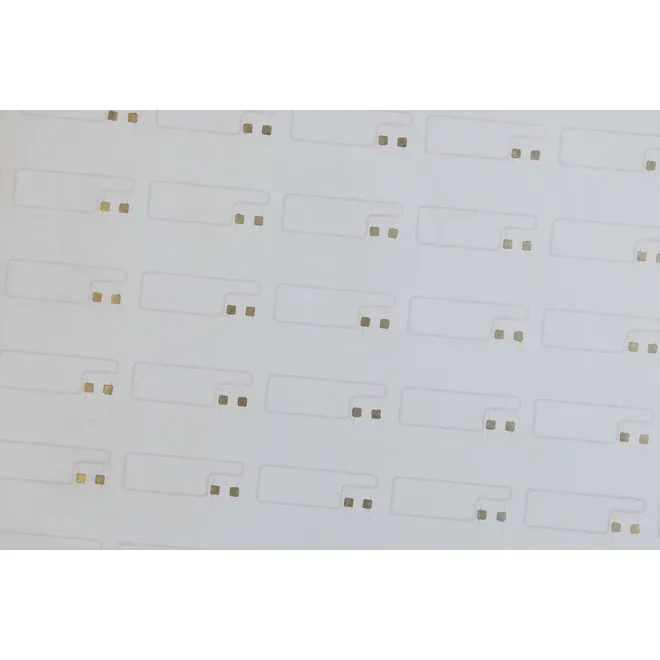
Two visible pads mark each connection location. The photo does not identify a CPU chip or a supplied operating system.
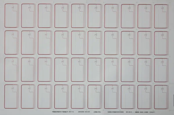
40 pictured positions. Count and arrangement describe this reference photograph; the order drawing specifies the sheet dimensions and pitch.
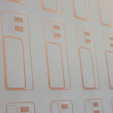
The close-up shows the expanded antenna-end regions used as a connection reference.
Technical documents
The PDF summarizes the four methods and sourced construction references. The original manufacturer documents explain CPU interfaces and inductive coupling.
Download CPU inlay technical reference ↓PDF · version 15 September 2026 · technical reference
Custom orders & samples
Your selections will be included in the inquiry draft. Add the module part number, drawing, quantity and delivery destination on the next page.
The quotation identifies module inclusion, substrate, sheet dimensions, thickness, MOQ and lead time.
Sample ordering terms →Dual-interface describes contact and contactless access to one compatible CPU chip. A combi card instead combines independent chips or functions. Two RF bands also describe a different architecture. Specify the CPU module and both reader interfaces before choosing the antenna connection.
A soldered design makes a direct electrical joint from the antenna ends to the module. An inductive design uses a module coil and a matching coupling region on the card antenna, with no galvanic connection between them. The module package, coupling geometry and card stack must be matched; changing the bonding process alone does not convert one design to the other.
The quotation must state whether supply is an antenna sheet, a prelam or a module-equipped assembly. CPU part number, module package, memory, operating system and personalization are separate selections. A controller or module approval does not by itself certify the finished RFIDAK card for a payment or identity scheme.
May we use Google Analytics cookies to measure visits and inquiry actions? Your choice does not affect the contact form. Cookie details