RFID Card Inlays — LF, HF & UHF
RFID card inlays combine an antenna and chip before final card finishing. Compare LF, HF, UHF, multi-chip and dual-interface constructions by electronics…
Product selection · 9 catalog options
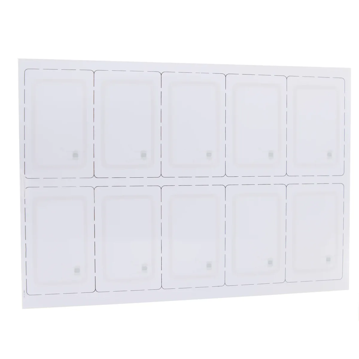
A card inlay is a semi-finished chip-and-antenna assembly for a card producer to integrate into a finished card. Specify the supplied stage, exact chip, sheet layout and complete card stack. LF, HF, UHF, multi-chip and dual-interface designs need different integration checks; a bare-inlay read does not establish performance after lamination and punching.
Explore the range
RFID card inlays combine an antenna and chip before final card finishing. Compare LF, HF, UHF, multi-chip and dual-interface constructions by electronics…
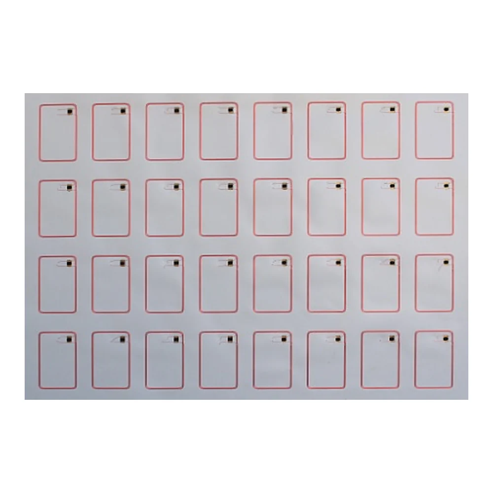
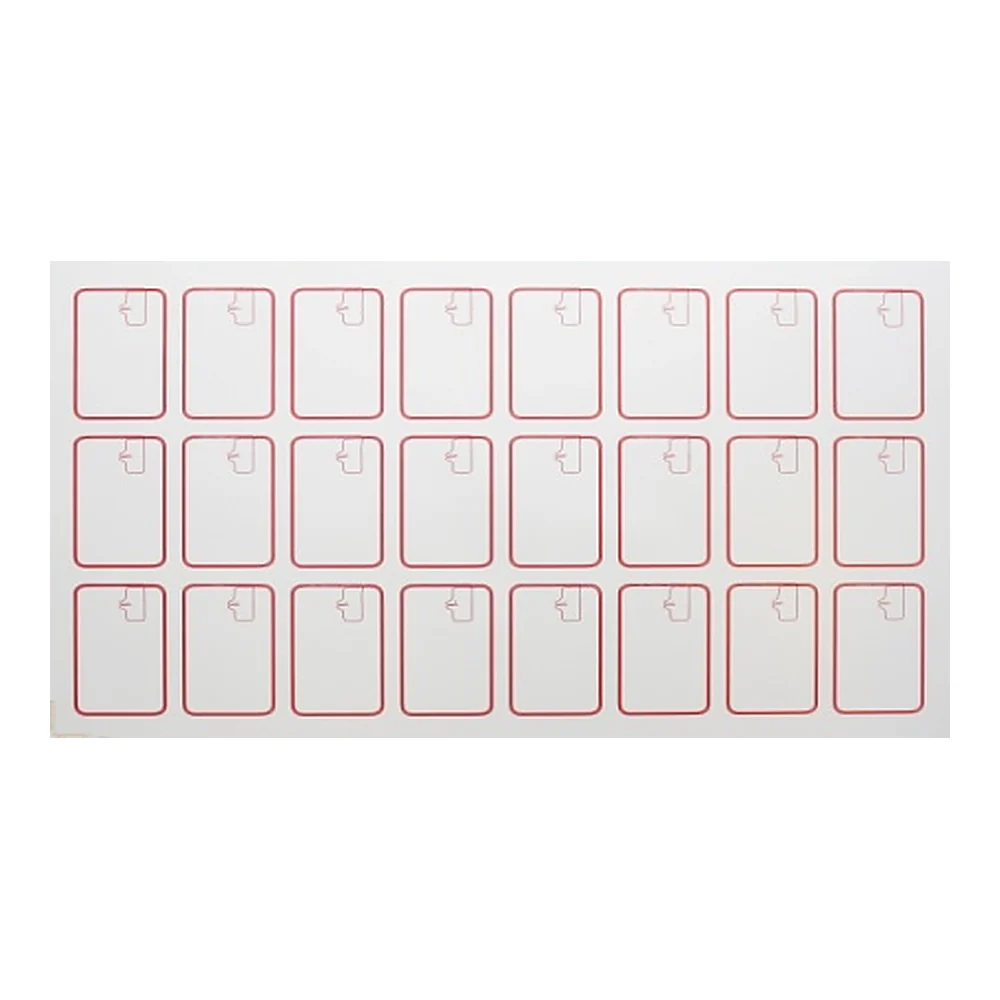
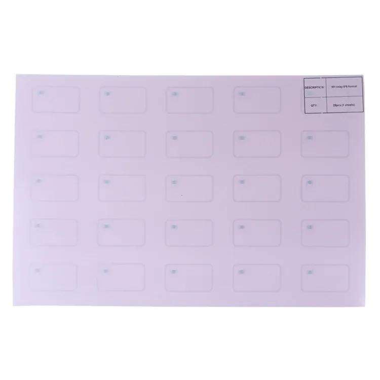
Compare 13.56 MHz HF card inlay chip specifications, 4 × 8 and 5 × 5 sheet examples, and a dimensioned COB stack. Download the technical reference and request samples.
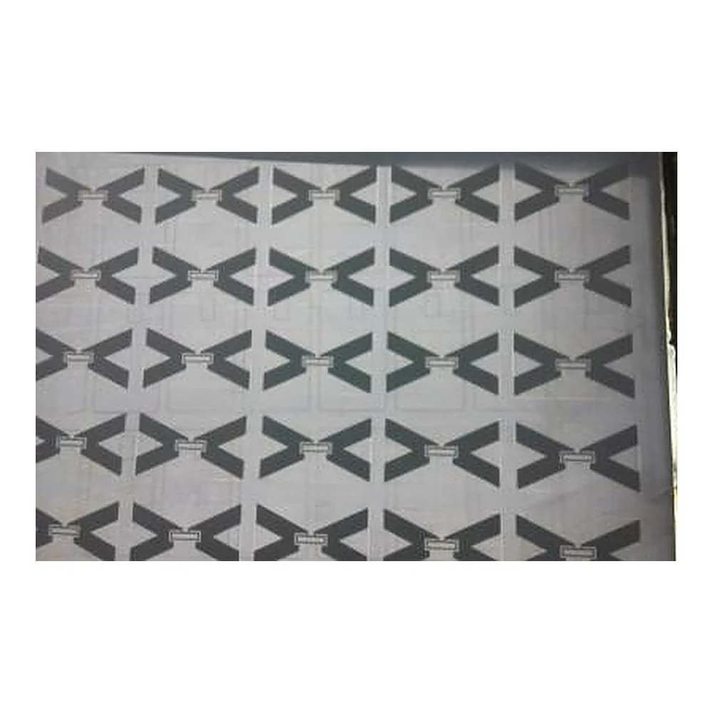
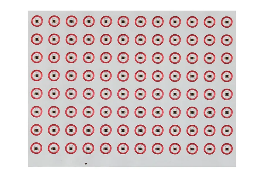
Compare UCODE 8, UCODE 9, M730 and legacy Monza R6 card inlay chip memory. See antenna-sheet photos, regional design guidance and a technical reference PDF.
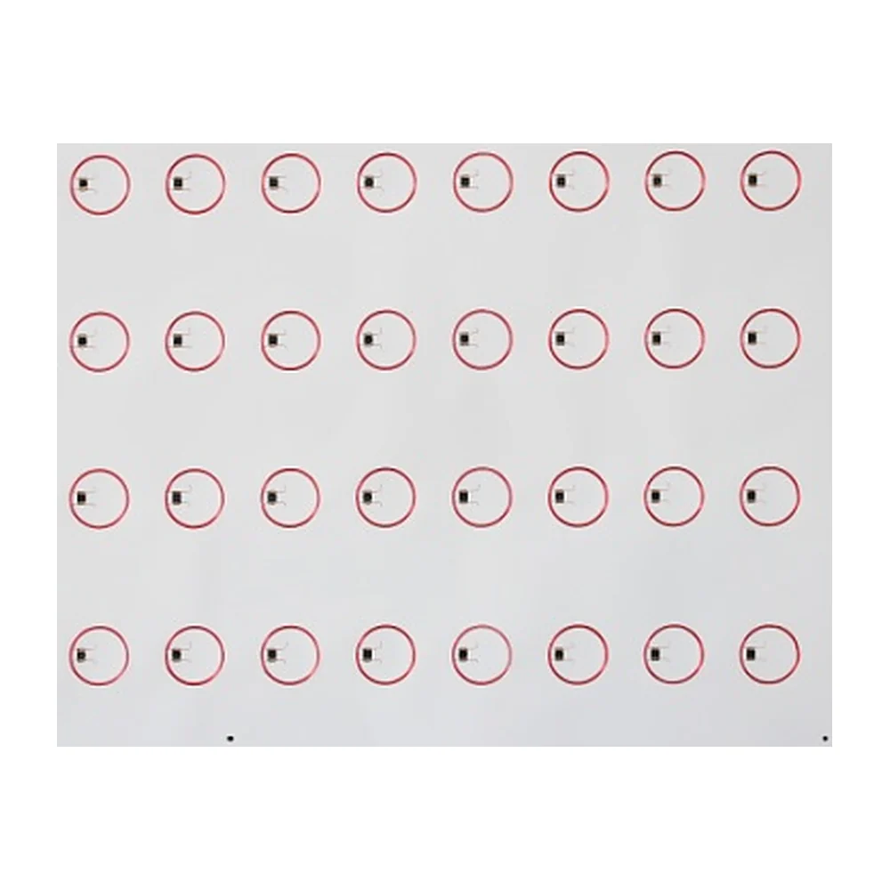
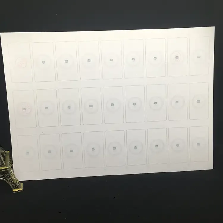
Compare EM4200, EM4305 and ATA5577C LF chip memory and read/write capabilities. See 3 × 7 and 2 × 5 card-inlay sheets, download technical references and request samples.
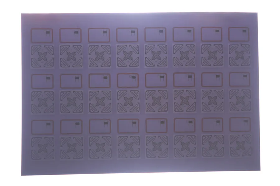
Compare EM4200 + NTAG213, EM4200 + DESFire EV3 and NTAG213 + UCODE 8 reference designs. See chip memory, separate-ID behavior, real sheet photos and technical sources.
Compare soldered, conductive-adhesive, pad and inductive-coupling CPU card inlay designs. View antenna sheets, dimensioned construction references and technical PDF.
Compare HF + HF and LF + HF multi-chip card-inlay references, separate memory and reader selection. View original sheet photos, package data and technical documents.
Irregular card inlays place a contactless antenna and chip within a non-standard outline for small cards, keychain shapes or encapsulated accessories. The…
Standard prelam references include 3 × 8 sheets at 295 × 480 mm and 4 × 8 sheets at 391 × 520 mm. Select sheet dimensions, card count, thickness and antenna…
From shortlist to sample
Send the chip, assembly stage, sheet drawing and complete card stack. We can review the integration, sample-sheet plan and acceptance requirements before quoting production.
Buying questions
Use the selected model’s information and an agreed sample test for the final decision.
Choose the supplied stage according to the processes you can perform. An inlay or prelam still needs a defined conversion process, which can include lamination, punching and module integration. A desktop card printer alone does not perform those stages. If you need printed cards ready for your issuance workflow, start with finished RFID cards instead.
No. Dual-frequency describes interfaces in different RF bands. Combi describes multiple chip functions according to the card design. A dual-interface CPU card provides contact and contactless communication through a compatible CPU module and antenna arrangement. Specify every chip and interface, including the stage at which the module is supplied or integrated.
Supply a drawing with sheet dimensions, usable area, card nests, pitch, registration marks, margins and punching clearance. Catalog examples include 2 × 5 through 6 × 8 layouts, but the actual stack and geometry need approval. Quote production sheets and usable inlays explicitly so a layout label is not mistaken for guaranteed finished-card yield.
Define the test operation, equipment or setup, acceptance limits, sampling or inspection coverage and position-level reject marking in the order. Ask for the records applicable to the supplied lot. An incoming chip response does not establish successful lamination, punching or final application performance; validate those separately on converted samples.
No. Contact and contactless interface support alone does not establish approval by a payment scheme, issuer or government program. Confirm the exact CPU module, operating system, application, integration method and required approvals with the responsible issuer. A module-family or Java Card reference is not a complete approved card specification.
Quote engineering samples, sample sheets, production sheets and usable inlay quantities separately. Confirm the exact chip supply, substrate, assembly stage, tooling and acceptance requirements, then agree MOQ and timing for that configuration. Keep conversion and finished-card acceptance in the schedule before releasing a repeat order.
Continue your selection
Define supply format, chip, stack and the card producer's integration responsibilities.
Separate module, interface and issuer requirements from the supplied prelam.
Agree usable positions, registration, defect marking and units in the quote.
Choose this route when you need finished card bodies rather than semi-finished assemblies.
May we use Google Analytics cookies to measure visits and inquiry actions? Your choice does not affect the contact form. Cookie details