Skip to content

Two RF bands · one card core

Dual-Frequency Card Inlays

LF + HF and NFC + UHF configurations

A dual-frequency card inlay combines two RF bands in one card core. An LF + HF design can support a 125 kHz reader and a 13.56 MHz application; an HF + UHF design can combine NFC interaction with an EPC reader. The discrete-chip examples below have separate identifiers and memory. Both reader functions must be checked in the final laminated card.

RF-band pairings
LF + HF · HF + UHF
Technical comparison
3 discrete-chip reference combinations
Supply form
Card-inlay / prelam assembly defined by drawing
Download technical reference (PDF) ↓
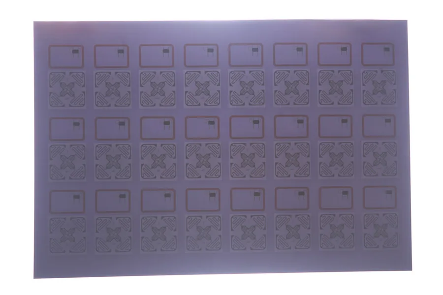
Sheet showing three rows of eight paired groups, each with a rectangular loop above a square patterned antenna.
24 paired antenna groupsOriginal sheet photograph · exact chips are not labelled · open full image ↗

Technical overview

Specify each band, chip and reader output.

The RF band tells you which reader is needed. The chip protocol and data format determine what that reader can do.

LF + HF
125 kHz + 13.56 MHz. Compare EM4200 with NTAG213 or MIFARE DESFire EV3. EM4200’s IC operating range is 100–150 kHz; the finished coil is designed for the target reader.
HF + UHF
13.56 MHz + a regional UHF band. NTAG213 provides NFC Type 2; UCODE 8 provides EPC Gen2v2 / ISO 18000-63. Its 840–960 MHz IC range is not a finished-card read-range specification.
Memory relationship
Separate chips have separate memory in the examples below. Link their identifiers in the issuing system when both functions belong to one credential.
Sheet evidence
3 × 8 paired groups are visible in the main photo. This count does not establish a chip model, sheet size or stocked layout.
Mechanical definition
The assembly drawing specifies substrate, sheet pitch, chip placement, antenna boundaries, thickness and tolerances for the chosen combination.

Chip-level comparison

Three combinations. Different jobs and memory.

These three combinations compare documented chip capabilities for design discussion. They are engineering references, not prequalified RFIDAK stock models. The quotation and approved drawing identify the supplied chips, antennas and card construction.

01

LF + HF · engineering reference

EM4200 + NTAG213

Existing LF identification plus an NFC phone-link function.

Review this combination →
EM4200 + NTAG213 per-chip frequency, protocol and memory
ChipFrequencyReader interfaceMemory & identifier
EM4200125 kHz design; IC range 100–150 kHzEM4100/4102-compatible formats; variant-dependent encoding128-bit ROM with 64 / 96-bit options; read-only. Manchester 64 carries 40 data bits.
NTAG21313.56 MHzISO/IEC 14443-A; NFC Forum Type 2144 bytes user memory; factory-programmed 7-byte UID.

The LF reader needs the selected EM encoding. Store the NFC link as an NDEF record; its overhead uses part of the 144-byte user area. The two ICs have separate identifiers.

02

LF + HF · engineering reference

EM4200 + MIFARE DESFire EV3

A migration credential for an existing LF system and a separately configured DESFire application.

Review this combination →
EM4200 + MIFARE DESFire EV3 per-chip frequency, protocol and memory
ChipFrequencyReader interfaceMemory & identifier
EM4200125 kHz design; IC range 100–150 kHzEM4100/4102-compatible formats; variant-dependent encoding128-bit ROM with 64 / 96-bit options; read-only.
MIFARE DESFire EV313.56 MHzISO/IEC 14443-A parts 1–4; application and key configuration required2 / 4 / 8 / 16 kB nonvolatile memory, selected by part number.

Specify the DESFire memory variant, application files and keys. Sharing one card does not transfer LF permissions to the DESFire system.

03

HF + UHF · engineering reference

NTAG213 + UCODE 8

NFC phone interaction plus a UHF identification workflow using an EPC reader.

Review this combination →
NTAG213 + UCODE 8 per-chip frequency, protocol and memory
ChipFrequencyReader interfaceMemory & identifier
NTAG21313.56 MHzISO/IEC 14443-A; NFC Forum Type 2144 bytes user memory; factory-programmed 7-byte UID.
UCODE 8840–960 MHz IC input; antenna and reader band specified separatelyEPC Gen2v2 / ISO/IEC 18000-63128-bit EPC + 96-bit factory-locked TID; 0 separate user bits. UCODE 8m is a different variant.

Choose the UHF antenna for the reader’s regional band. The NTAG UID and UCODE TID are distinct; a writable EPC can be mapped to the same application record.

Application fit is an engineering interpretation of the documented IC interfaces. The three examples use discrete chips; “dual-frequency” alone does not define every possible chip architecture or its memory relationship.

Reader-output example

One physical card can have two different identifiers.

EM4200 + NTAG213 engineering example. Check the value each system actually receives.

125 kHz reader

EM4200 → LF identifier

The EM4200 Manchester 64 version transmits 40 data bits inside a 64-bit frame. The access reader may format or truncate that value before returning a card number.

13.56 MHz NFC reader

NTAG213 → UID or NDEF content

NTAG213 has a separate factory-programmed 7-byte UID and a 144-byte user area for data such as an NDEF link. Writing that link does not rewrite the chip UID or the EM4200 ROM.

One record in your issuing system

An application can associate the returned LF identifier and the NFC identifier or link token with one credential record. That association belongs to the issuing system; these two chips do not automatically share memory, permissions or revocation.

For the EM4200 frame, see the manufacturer datasheet page 6. For the NTAG213 UID, see section 8.5.1 of the NXP datasheet. Both are linked in technical documents.

Original sheet evidence

See the antenna arrangements at a useful scale.

Two photographs show physical sheets. Their visible geometry helps discuss a layout, while chip identity and millimetre dimensions come from the approved drawing.

Sheet showing three rows of eight paired groups, each with a rectangular loop above a square patterned antenna.

24 paired antenna groups

Three rows of eight paired groups are visible. The photo has no readable chip or band label, so it documents the arrangement rather than a specific combination in the table.

Open full image ↗
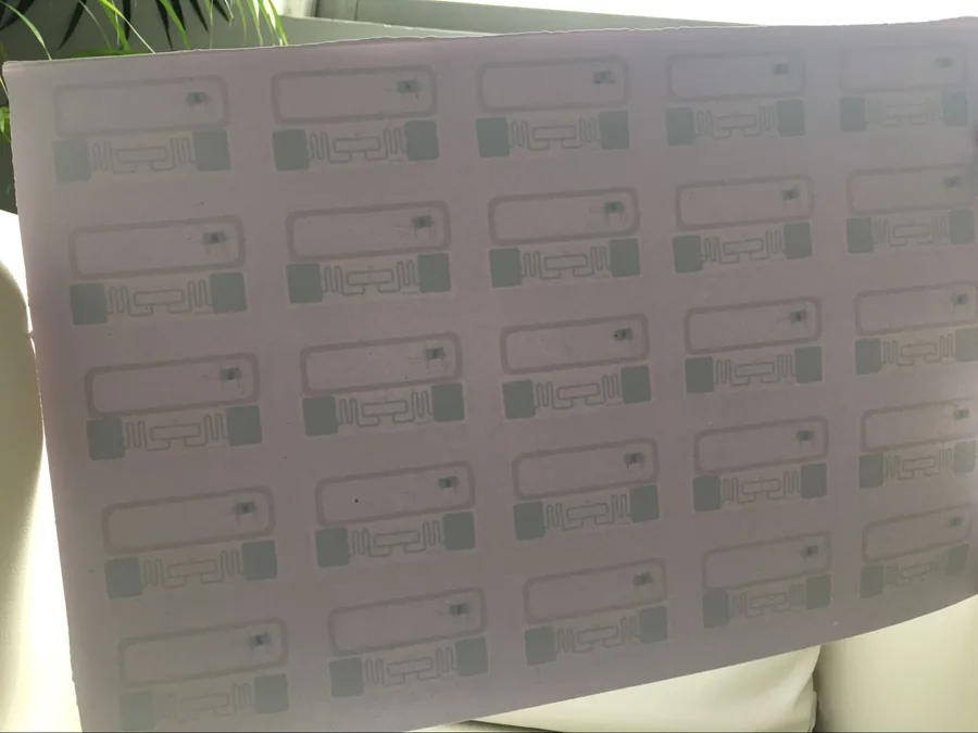
An angled sheet photograph with repeated rectangular loops and elongated antenna patterns underneath.

Loop and elongated-antenna sheet

This original photograph shows another arrangement in the existing gallery. The angle and sheet edges do not establish an exact supplied size, thickness or chip identity.

Open full image ↗
View the original layout illustrations and historical source
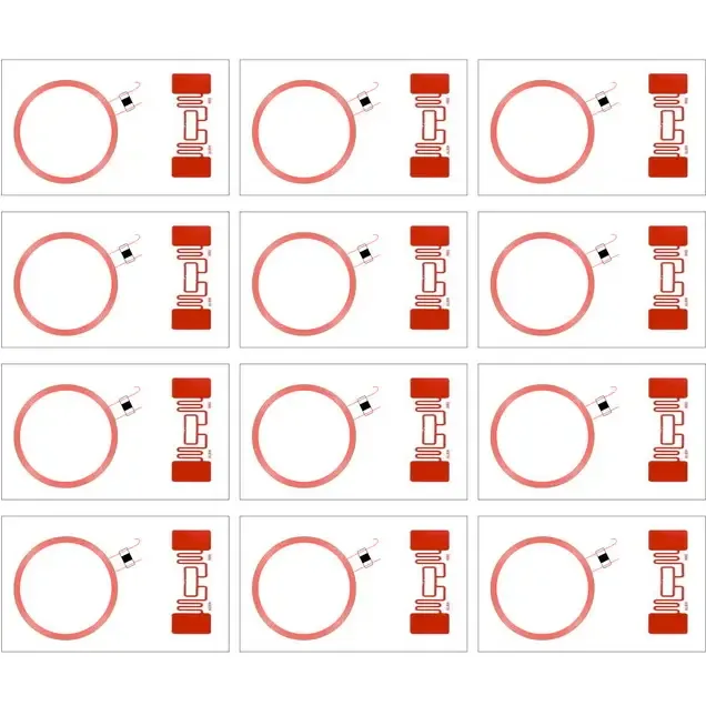
Illustration of twelve outlined positions in four rows and three columns, each containing a circular loop and a narrow antenna pattern.

Twelve-position layout illustration

An illustrative 4 × 3 arrangement from the original gallery. This is a drawing, not a measured production sheet or proof of a particular chip combination.

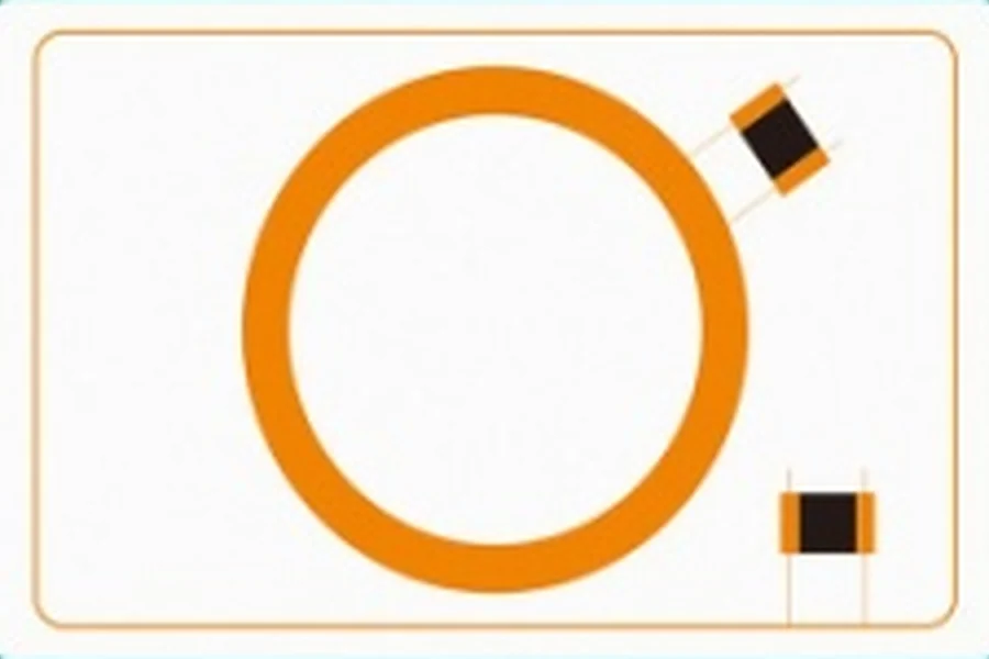
Historical schematic containing a large circular loop inside a rectangular loop, with two dark component symbols.

Historical composite construction sketch

ACT Trinnovation, Q4-2017 presentation, slide 19, image31.jpeg. A composite-layout illustration without chip names, frequencies or dimensional tolerances.

Technical documents

Share the comparison with your card integrator.

The technical reference collects the three combinations, identifier example and evidence scope. Use the original IC documents for memory maps, commands and electrical conditions.

Download dual-frequency reference ↓

PDF · version 15 September 2026 · engineering reference

Custom orders & samples

Which two reader functions does your card need?

Select a reference combination or specify your own. Add both reader models, application requirements, sheet drawing, quantity and destination on the inquiry page.

The quote will identify the exact IC variants, antenna layout and supplied assembly, with sample charges, MOQ and lead time. Sample acceptance should cover both reader functions after lamination and punching.

Sample ordering terms →

These choices identify a design request. The finished assembly is confirmed during technical review.

Dual-frequency card-inlay questions

Do both readers see the same card number?

Not automatically for the discrete-chip examples shown. EM4200 has factory-programmed ROM; NTAG213 has its own 7-byte UID; UCODE 8 has a factory-locked TID and writable EPC. Your issuing system can map the values to one record. Agree exactly which value each reader returns, including formatting, before creating the mapping.

Is ISO 14443 plus ISO 15693 a dual-frequency design?

Both interfaces operate at 13.56 MHz. Combining them is a same-band, multi-protocol design, not two different RF bands. A dual-interface CPU card is another distinction: it provides contact and contactless interfaces. Specify the required reader interfaces rather than treating these names as interchangeable.

Can a phone read the LF or UHF side of these examples?

An NFC phone can interact with the 13.56 MHz NTAG213 side when the phone and encoded content support the intended action. It does not read EM4200 at 125 kHz or UCODE 8 through its UHF interface using the phone’s NFC radio. Those functions need their corresponding readers. A DESFire application also needs the appropriate commands, keys and software.

WhatsAppGet a Quote